Nov . 13, 2024 05:06 Back to list
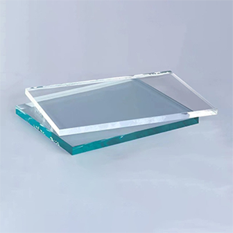
glass etch bath
The Importance of Glass Etch Bath in Semiconductor Fabrication
In the realm of semiconductor manufacturing, precision and detail are of utmost importance. One essential process that contributes to achieving these standards is the glass etching technique, particularly the use of the glass etch bath. This process plays a crucial role in creating intricate patterns and structures on glass substrates, which are vital in the fabrication of various electronic components.
A glass etch bath typically involves a chemical solution that selectively removes material from the glass surface. This etching solution can be made from a variety of chemicals, often including hydrofluoric acid or other specialized compounds designed to interact with the silica in glass. The primary purpose of the etch bath is to function as a mask, allowing manufacturers to create precise and well-defined patterns that are crucial for the functionality of devices such as photomasks, sensors, and display technologies.
The process begins with the application of a photoresist layer on the glass substrate. This layer is then exposed to ultraviolet light through a patterned mask, which allows for selective curing of the photoresist. After developing the photoresist, the glass substrate is immersed in the etch bath. The exposed areas of the glass, now free of photoresist, are etched away by the chemicals in the bath, resulting in the desired pattern.
glass etch bath

The importance of controlling the conditions of the etch bath cannot be overstated. Parameters such as temperature, concentration of the etching solution, and duration of exposure directly influence the etching rate and the quality of the final pattern. A well-maintained etch bath ensures that the etching process yields high-resolution features while minimizing any undesired etching or defects.
Additionally, safety precautions are paramount when handling etching chemicals due to their corrosive and toxic nature. Proper personal protective equipment (PPE) should always be used, and protocols for safe disposal of etching solutions must be established to protect both workers and the environment.
In conclusion, the glass etch bath is a vital component in the semiconductor fabrication process. Its ability to create intricate and precise patterns on glass substrates significantly contributes to the advancement of electronic devices. As technology continues to evolve, the role of precise glass etching and the refinement of etch baths will remain critical in pushing the boundaries of innovation in the semiconductor industry.
-
Safety and Style with Premium Laminated Glass Solutions
NewsJun.24,2025
-
Reinvents Security with Premium Wired Glass
NewsJun.24,2025
-
Premium Float Glass Line for Modern Architecture
NewsJun.24,2025
-
Low Emissivity Glass for Energy-Efficient Architecture
NewsJun.24,2025
-
High-Performance Insulated Glass Solutions for Modern Architecture
NewsJun.24,2025
-
Elevates Interior Style with Premium Silver Mirror
NewsJun.24,2025
Related PRODUCTS